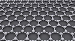
Graphene possesses interesting optical, mechanical, and thermal properties for all sorts of applications, including flexible electronic circuits and electromagnetic-interference (EMI) shielding. It also holds great promise in the RF/microwave arena, with carrier mobility that’s about 100 times greater than silicon and about 10 times the speed of indium-phosphide (InP) substrate materials. So far, graphene has been used in millimeter-wave mixers and radiometers, but its benefits could make an impact on many other millimeter-wave and even terahertz-frequency components and devices.
To demonstrate some of the capabilities of this material, Jeong-Sun Moon and fellow researchers from HRL Laboratories LLC, Malibu, Calif., explored the fabrication and performance of different graphene field-effect transistors (GFETs). Starting with a gate length of 1 μm, the experimenters achieved dc amplifier gain of 100 for an input signal level of –12.3 dBm at 30 GHz. By cutting the gate length in half to 0.5 μm and using a source-to-drain spacing of 1 μm, the devices yielded responsivity of 33 V/W at frequencies as high as 110 GHz. The researchers estimated a 3-dB bandwidth of approximately 50 GHz for the smallest of these devices.
As linear detectors, the GFETs showed the ability for direct detection of RF power at 170 and 214 GHz when operating at zero bias, with drain-source and gate-source voltage of 0 V dc. When using nominal low bias voltage levels, and comparing the dynamic range of these GFET detectors to existing silicon-germanium (SiGe) detectors, the GFET detectors achieved RF power-detection dynamic range of better than 40 dB (from –50 to –9 dBm) at 30 GHz (with 0-V dc drain-to-source voltage and 0.5-V dc gate-to-source voltage). In a comparison with silicon CMOS detectors, the researchers projected that these GFET detectors could deliver the 40-dB detection range at frequencies through 110 GHz.
Their work in graphene as a semiconductor material included fabrication of graphene heterostructure diodes and design of a 200-GHz graphene diode detector on a sapphire substrate. Estimates showed the device was capable of noise equivalent power (NEP) of about 8 pW/Hz0.5 and responsivity of 1020 V/W, both parameters at 200 GHz. Such research work on graphene FETs and lateral heterostructure diodes points to great promise for graphene as a semiconductor building-block material for millimeter-wave and terahertz applications.
See: “Graphene and Lateral Heterostructure for THz Imaging,” IEEE Transactions on Terahertz Science and Technology, May 2015, p. 344.
