Download this article as a .PDF
Power amplifiers for modern telecommunication systems often must deliver a wide range of output power levels with high efficiency and high linearity. Generally, when designed for the highest power levels with maximum available efficiency, PAs in cellular base stations tend to operate less efficiently at lower power levels, consuming excessive dc power at lower power levels.
In such wireless systems with wide bandwidths and high data rates, transmitted signals are typically characterized by high peak-to-average power ratio (PAR) due to wide and rapid variations of the instantaneous transmit power. Therefore, it is a real challenge to design a base-station PA with high efficiency not only at maximum output power, but also at lower power levels typically 6 dB or less than the maximum output levels, in a configuration with relatively small size and low cost.
By using GaN HEMT technology and innovative Doherty architectures, however, average efficiencies of 50 to 60% and average output powers to 100 W can be achieved that significantly reduce transmitter power consumption. GaN HEMT technology features many benefits, including high breakdown voltage, high current density, high transition frequency (fT), low on-state resistance, and low parasitic capacitance. These characteristics result in high output power, wide bandwidth, and high operating efficiency.
The high power density makes it possible to construct physically compact designs at high output power levels, while high dc-supply voltage operation and low parasitic output capacitance result in higher load impedances for ease in obtaining wide operating bandwidths. A drain-to-source breakdown voltage in excess of 150 V dc enables rugged operation at 50 V, regardless of drive level or harmonic load environment.
Sumitomo GaN HEMT technology can provide high-gain operation of a packaged device at output power levels to 300 W for operating frequencies over 8 GHz and beyond for radar applications and can provide excellent, reliable performance for high-power wireless cellular communications transmitters. The progress in power density for the current generation of active devices at 5 W/mm makes it possible to reach 10 W/mm at 50 V dc. The use of silicon-carbide (SiC) substrate material provides excellent thermal management at high power levels.
For a conventional Doherty amplifier with a quarter-wave impedance transformer and a quarter-wave output combiner, efficiency of 31% was measured for power levels backed off 6 to 7 dB from a saturated output-power level of about +43 dBm, for a frequency range of 1.5 to 2.14 GHz.1 To improve the broadband performance of a conventional Doherty amplifier, an output network can be composed of two quarter-wave impedance inverters with reduced impedance transformation ratios.2 For broadband combining, an output quarter-wave transmission line with fixed characteristic impedance can be replaced by a multiple-section transmission line with different characteristic impedances and different electrical lengths for its multiple sections across a frequency range of 2.2 to 2.96 GHz.3
High peak power of 500 W was achieved across the lower frequency band of 760 to 960 MHz using a modified combining scheme with two quarter-wave lines in the peaking path.4 For an asymmetric Doherty architecture, saturated power of more than 270 W and linear gain of more than 13 dB with drain efficiency of more than 45% at 8-dB back-off were achieved from 2.5 to 2.7 GHz.5 An average power of 85 W with peak power of 470 to 570 W and relatively flat average efficiency of 45 to 49% was achieved across the frequency band of 1.8 to 2.2 GHz for a single-carrier WCDMA signal with PAR of 10 dB.6
Packaged Device
High-power GaN HEMTs can be achieved with large gate periphery resulting in higher power capability for a given package size compared to some other active device structures. The corresponding increase in gate-source capacitance when multiple basic device cells are connected in parallel reduces the optimum input impedance to very low values, close to one or a few tenths of an ohm. Therefore, a low-loss matching network is required inside the package to transform the impedance from the package lead reference plane to the device die reference plane.
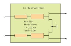
For practical use, a packaged GaN HEMT power device should provide reasonably high (not less than 1 Ω) input impedance with a sufficiently low quality (Q) factor to provide flat performance over a required frequency bandwidth. Depending upon the space available within the device package and providing sufficiently wide operating bandwidth to 40%, a two-step microstrip line on a high-permittivity substrate might be considered (Fig. 1) for a dual-path package where two 180-W GaN HEMT dice are attached in parallel.
Such a two-stepped microstrip-line transformer for each device can transform the device input impedance of a few tenths of an ohm to an input impedance of several ohms with a flat or a custom required response. The latter will also feature high return loss for each device across the entire frequency bandwidth from 1.8 to 2.2 GHz for this particular application.
Modified Doherty Amp
For a high-power amplifier with very low output impedance, the width of the matching microstrip line will be very wide compared to its length. The overall size of the matching circuit, including an offset line to create an open-circuit condition when the peaking amplifier (PA) is turned off, and a quarter-wave transforming line, becomes sufficiently large; it becomes difficult to physically connect the output of the peaking amplifier directly to the main amplifier path. Therefore, for convenience of implementation, a classical Doherty amplifier configuration can be modified by including of an additional half-wave line at the output of the PA.
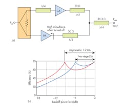
Figure 2 shows the schematic diagram of a modified two-stage Doherty amplifier configuration where a half-wave line is connected to the output of the PA and a quarter-wave line is included at the input of the main or carrier amplifier (CA) for phase compensation. This configuration is characterized by the same two peak efficiency points, at saturation and -6 dB power back-off, similar to the classical two-stage Doherty amplifier (DA) shown in Fig. 2b.
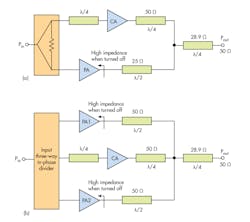
There is a possibility to extend the region of high efficiency over a wider range of output powers if the CA and PAs are designed to operate with different output powers, smaller for the CA and larger for the PA. For instance, for a power-division ratio 1:2, the transition point with maximum drain efficiency corresponds to the back-off power level of -9.5 dB from peak output power, as shown in Fig. 2b. In this case, the characteristic impedance of the half-wave line is 25 Ω, corresponding to the load impedance required for the PA; the characteristic impedance of the combining quarter-wave line is 28.9 Ω, as shown in Fig. 3a.
For packaged devices, where it is difficult to choose the proper power ratio between the devices, it is convenient to use identical power amplifiers which can compose ideally the multi-way Doherty architecture where one carrier power amplifier is in parallel with multiple peaking amplifiers. As a result, a 1:2 asymmetric two-stage Doherty structure can be transformed to a modified three-way asymmetric Doherty configuration with one CA path and two identical PA paths when device sizes for the CA and both PAs (PA1 and PA2) are equal, as shown in Fig. 3b.
Here, the half-wave line in each PA path can be split into two quarter-wave lines, each having its own characteristic impedance for the corresponding impedance transformation when the required load impedance for peaking device is sufficiently small.
Three-Way Doherty Amp
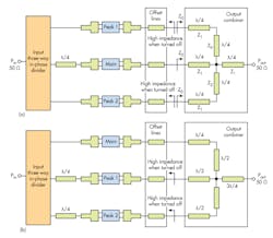
Figure 4a shows the block schematic of a three-way asymmetric Doherty amplifier configuration based on three dual-device packaged transistors. Each has a pair of 180-W GaN HEMT devices with internal input matching microstrip-line networks, where the output combiner includes one quarter-wave microstrip line in a CA path, two quarter-wave microstrip lines in each identical PA path, and one combining quarter-wave microstrip line. Each amplifying path includes the packaged device of the same die size, with input and output matching circuits using microstrip lines.
Offset lines are necessary to provide open-circuit conditions at their ends for PAs when they are turned off. Two quarter-wave microstrip lines with different widths required for the corresponding impedance transformation translate this open-circuit condition in each peaking path to an open circuit seen by the carrier path at output power levels lower than -9 dBc at a common node in the output combiner.
For example, for identical amplifiers having optimum load impedance Z0 = 12 Ω each and Z2 = RL = 50 Ω, where RL is the standard 50-Ω load impedance, Z1 = (Z0Z2)0.5 = 24.5 Ω and Z3 = (Z2RL)0.5/(3)0.5 = 28.9 Ω. There may be different combinations of the characteristic impedances between quarter-wave microstrip lines in the output combiner. The quarter-wave microstrip line in the input path of the carrier amplifier is used to compensate for the delay of the output combiner.
Another circuit implementation of a high-power asymmetric three-way GaN HEMT Doherty amplifier to operate across the frequency bandwidth of 1.8 to 2.2 GHz, where a half-wave microstrip line is included in the load network of each identical peaking path for better flexibility in practical implementation is shown in Fig. 4b, while providing sufficient bandwidth capability at the same time. Here, microstrip line (l/4 + l/2) with a total electrical length of 270 deg. provides the corresponding impedance transformation at significant power backoff and the quarterwave microstrip line in each input path of the peaking amplifiers compensate for the delay provided by the output combiner. The broadband output impedance transformation with 50-Ω load is provided by a Klopfenstein taper having an electrical length of 270 deg. at the center bandwidth frequency.
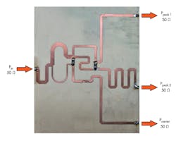
The input three-way in-phase power divider, with layout shown in Fig. 5, was implemented on a 20-mil-thick RO4350 circuit substrate from Rogers Corp. which was also used to implement the entire Doherty amplifier circuit. It includes a transforming quarter-wave line; an asymmetric 1:2 two-way Wilkinson divider to split power between the two paths, one with the carrier and first peaking amplifiers and the other with the second peaking amplifier; a symmetric two-way Wilkinson divider to equally split power between the carrier and first peaking amplifiers; an additional 50-Ω quarter-wave microstrip line in carrier path; and three equal-length 50-Ω connecting microstrip lines in the carrier and two peaking paths. To provide flatter response over the entire frequency bandwidth, additional input offset lines were connected to the outputs of the input in-phase combiner.
Test Results
A test board for a three-way Doherty amplifier was fabricated on 20-mil-thick RO4350 circuit material from Rogers Corp. The three-way amplifier is based on three dual-path GaN HEMT devices in metal-ceramic flange packages with a pair of 180-W GaN HEMT die and internal input matching network each, according to the block schematic diagram shown in Fig. 4b. The input three-way divider, input and output matching circuits, offset lines, output combiner, and gate and drain bias circuits (having bypass capacitors on their ends) are fully based on microstrip lines of different electrical lengths and characteristic impedances. Special care was taken for device implementation process in order to minimize the output lead inductances of the packaged GaN HEMT device.
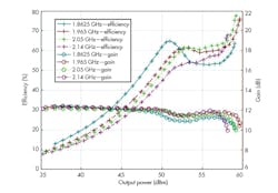
Peak output power of +59.5 dBm was measured at 2-dB gain compression (P2dB) and peak efficiency of 78% was measured with linear flat power gain of about 12 dB, for a supply voltage of 55 V dc and a frequency range of 1.8 to 2.2 GHz (Fig. 6). From these test results, it follows that drain efficiency of greater than 50% at 8-dB power back-off can be achieved. This means that, for a 20-MHz LTE signal with 8-dB PAR, average power of 120 W can be obtained with a drain efficiency of equal or greater than 50% over most of the frequency range. This is the best result in industry in terms of power gain flatness, output power, and back-off efficiency achieved over a wide frequency bandwidth of 1.8 to 2.2 GHz.
High backoff efficiency, above 50%, and high-power gain, about 12 dB, can be achieved from 1.8 to 2.2 GHz at an exceptionally high output-power level of about 1 kW corresponding to the 2-dB gain compression point. In addition, the modified asymmetric Doherty amplifier offers the capability to operate with digital predistortion (DPD) in order to meet stringent spectral mask requirements.
James Wong, RF PA Specialist
Naoki Watanabe, Senior RF Engineer
Andrei Grebennikov, RF PA Specialist
Sumitomo Electric Europe Ltd., 220 Centennial Park, Elstree, Hertfordshire, WD6 3SL, UK
References
1. K. Bathich, A.Z. Markos, and G. Boeck, “A wideband GaN Doherty amplifier with 35% fractional bandwidth,” in Proceedings of the 40th European Microwave Conference, 2010, pp. 1006-1009.
2. K. Bathich, D. Gruner, and G. Boeck, “Analysis and design of dual-band GaN HEMT based Doherty amplifier,” in Proceedings of the 6th European Microwave Integrated Circuits Conference, 2011, pp. 248-251.
3. G. Sun and R.H. Jansen, “Broadband Doherty power amplifier via real frequency technique,” IEEE Transactions on Microwave Theory & Techniques, Vol. MTT-60, January 2012, pp. 99-111.
4. D.Y. Wu, J. Annes, M. Bokatius, P. Hart, E. Krvavac, and G. Tucker, “A 350 W, 790 to 960 MHz wideband LDMOS Doherty amplifier using a modified combining scheme,” in 2014 IEEE MTT-S International Microwave Symposium Digest, pp. 1-4.
5. N. Yoshimura, H. Umeta, N. Watanabe, H. Deguchi, and N. Ui, “A 2.5-2.7-GHz broadband 40W GaN HEMT Doherty amplifier with higher than 45% drain efficiency for multi-band application,” in 2012 IEEE Radio and Wireless Symposium Digest, pp. 53-56.
6. R. Hajji, L. Ledezma, G. Burgin, J. Gengler, and T. Langdon, “85-W Pavr, 500W peak power, 1.8-2.2-GHz wideband GaN Doherty power amplifier,” in 2017 IEEE MTT-S International Microwave Symposium Digest, pp. 1-4.

