Understanding Ultra Narrowband Modulation

Modulation advances have fueled more efficient use of bandwidth, although conventional modulation formats still require allowance for upper and lower sidebands around the carrier frequency.
What is Ultra Narrowband Modulation?
Ultra narrowband modulation, however, is an efficient form of transmitting information without using sidebands. The modulation format, which is also known as very minimum sideband keying (VMSK) or minimum sideband (MSB) modulation, has been in development since 1985. Although stalled since that time due to the lack of practical filters, the modulation method is now available to system developers through the use of filtering techniques with zero group delay.
Ultra Narrowband Modulation vs. Traditional Modulation
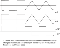
A review of more conventional modulation formats, such as frequency modulation (FM) and phase modulation (PM), may help when attempting to understand MSB modulation. For example, in conventional modulation formats, changes in frequency and phase occur gradually (right-hand side of Fig. 1), compared to the abrupt changes in frequency and phase of MSB modulation (left-hand side of Fig. 1).
Mechanics of MSB Digital Modulation
MSB digital modulation utilizes a coded baseband with abrupt edges; that is, the rise/fall times are as abrupt or near zero as possible. Some resistive-capactive (RC) rise time is inevitable, due to slew rates in integrated circuits (ICs) and other parts of the transmitter/receiver circuitry. In practice, these changes occur during one cycle of the intermediate frequency (IF).
Frequency Calculations in Modulation
For example, the frequency resulting from a modulating input signal is F = Fcarrier + Δf, where the modulation frequency, Δf, can be calculated from the basic relationship of ωt = φ = 2πft. The modulation frequency can also be rewritten in derivative form as Δf = Δφ/2πt. The rise/fall time, t, is fixed by the circuit parameters. During rise/fall times for abrupt phase modulation, there is a large Δφ/Δt which causes large Δf (almost infinite) for a very short duration (about 1 cycle at RF). At all other times, Δφ is zero and the frequency is constant at F = Fcarrier. A phase detector using Fcarrier as a phase reference will detect the phase changes as positive and negative voltages, but will ignore large Δf. In this case, consider Δφ as being zero for most of the bit (information) period.
The situation is different for the waveform in the right-hand side of Fig. 1. In that case, Δφ has a finite value and lasts for the entire period of the phase change. There is a definite change in frequency for the phase change period. Armstrong2 used this concept to produce FM from PM in 1936. If Δφ/Δt is caused by a sine wave, the resulting FM is a cosine wave, since FM is the derivative of PM.
The abrupt phase change and resulting frequency change in the left-hand side of Fig. 1 was noted by Professor Howe in 1939.1 The observation was not applied since digital-modulation techniques were not in use at that time, and the filters needed to take advantage of the abrupt phase changes were not available.
Filter Requirements for Ultra Narrowband Modulation
Any bandpass filter used at the transmitter for ultra narrowband (MSB) modulation must exhibit zero group delay to pass the instantaneous phase changes, though it may lack the bandwidth required to pass instantaneous changes in frequency. To all intents and purposes, there is no measurable frequency change, but there is a phase change in the carrier that is maintained constant between the rise and fall times. A conventional, or Nyquist filter, has group delay and rise time. This causes the phase modulation to spread out over time, and the result is FM (right-hand side of Fig. 1).
Vector Analysis of Sidebands
According to accepted practice using PM to generate FM (the Armstrong method), a carrier and upper and lower sidebands are required (Fig. 2).2
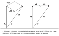
The vectors for the upper and lower sidebands counter-rotate in phase, reaching a maximum in either direction when they are at the same phase. The upper sideband (USB) is a signal higher in frequency than the carrier by an amount equal to the modulation frequency. The lower sideband (LSB) is lower in frequency than the carrier by the same amount. This gives rise to Bessel products, which are necessary to cause the vector V4 to shift in phase. There are three or more different frequencies involved to produce the phase shift, φ.3
The equivalents of the USB and LSB are seen as vectors V2 and V3 when using abrupt phase modulation. They must maintain the phase shift, φ, at a constant angle, hence they cannot rotate, but can only reverse. If they do not rotate, they are not at different frequencies, but at the same frequency as the carrier V1.
Abrupt phase-angle modulation does not require any frequencies other than the carrier. There are no Bessel products or other frequencies required to produce the phase shift. This is obvious from the mathematics. If the modulation frequency, Δf is equal to Δφ/2πt, and the change in the phase shift, Δφ, is zero, then Δf is zero. The level of the Jn Bessel products, as referenced from a Bessel function table, is determined by β = Δφ. If β = 0, there are no Bessel products other than the J0 product.3
When using a coded baseband to produce the rectangular waveform in the left-hand side of Fig. 1, and using 90-deg. abrupt phase modulation, the spectrum of Fig. 3 would result.
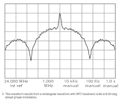
Non-return-to-zero (NRZ) information from a CMOS driver is used to avoid having an unfamiliar baseband code for this example (with a data rate of 270 kb/s using random data). The dome-shaped base of the spectrum is the sum of the Fourier frequencies associated with random NRZ data. Although the Fourier products are amplitude products only, they do appear using this modulation method. They do not cause any phase shift and can be reduced by zero-group-delay filtering.
When Bessel products are present, the phase angle is related to the level of the Bessel sidebands by the relationship 2J1 = sinφ (from ref. 3). If this relationship were to hold true for the Fourier products, the phase-detected output would decrease linearly with the decrease in the Fourier sinx/x product level. Using this formula to calculate the assumed decrease in phase angle, and comparing this with the actual detected output level, it can be seen that the detected phase angle has almost no change.
The Fourier products are sin/x/x products that can be ignored since they produce no PM. The measured phase angle output level from the phase detector is almost independent of these products as seen by the measured line. Calculated and measured results are show in Fig. 4.
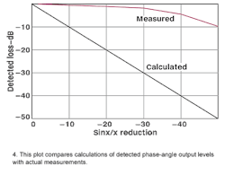
Adding several cascaded stages of zero-group-delay filtering does cause some loss, although optimum tuning will yield a higher output level than shown in Fig. 4.
Fourier sinx/x products have no relationship to the detected phase angle. The zero-group-delay filters used with MSB modulation have a bandwidth that is only 2 to 3 kHz wide, resulting in an excellent signal-to-noise relationship. The narrow filter bandwidth also makes it possible to pass a single frequency (J0), while rejecting the Fourier sinx/x sidebands.
The spectrum shown in Fig. 5 and 6 has a measured phase angle level, from the detector, that is only 2 dB less than the measured level when no filter is used.
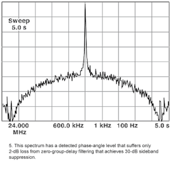
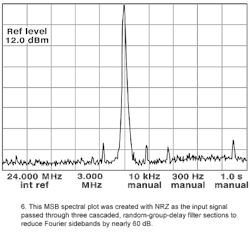
The zero-group-delay filter reduces the Fourier product levels by 30 dB. The level remains near that for the unfiltered signal, even when the Fourier sidebands are reduced further. Figure 6 shows Fourier sidebands that a reduced by nearly 60 dB using three cascaded filter sections, while the detected phase change output level is only reduced by 10 dB or less compared to Fig. 4. NRZ data was used as the input, with random data and zero group delay filtering to reduce the sinx/x Fourier products. There is some loss because the cascaded filter sections do introduce a small amount of group delay, which reduces the detected phase angle.
The Fourier sinx/x level has the characteristics of noise, the level of which varies with the bandwidth. The spectral plots of Figs. 3, 5, and 6 were created with different spectrum analyzer resolution bandwidths. Figure 7 shows two filters that use the crystal in the parallel mode as a large pure resistance for a single frequency at resonance (shunt and bridge).
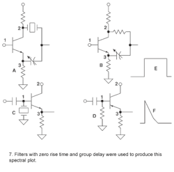
Figures 7(c) and 7(d) show the equivalent circuit while Figs. 7(e) and 7(f) show the impulse responses. These circuits have a rise time determined by other parts of the circuit, not by the crystal and the coupling capacitor. The crystal does not act as a bandpass device in the circuit, but passes the abruptly modulated input signal around it in the manner of an RF differentiator. The signal is passed via the capacitor, ignoring the resistor. For frequencies other than the single frequency at resonance, the circuit sees the reactance of the crystal as a load. The crystal acts as a capacitor in a capacitor voltage divider circuit, with other impedance values making it an integrator, not responsive to short bursts.
What is the performance of the crystal filter in terms of bandwidth efficiency? Bandwidth efficiency is defined as the bit rate per bandwidth, such as 2 b/s/Hz. Assuming the 2-to-3-kHz 3-dB bandwidth of the crystal filter, the bandwidth efficiency is very high. For a bit rate of 270 kb/s at that crystal filter bandwidth, the bandwidth efficiency is 100 b/s/Hz.
The signal-to-noise ratio (SNR) can be determined from the formula given by Feher.4:
SNR = β2C/N or
SNR = β2(bit rate/filter bandwidth)Eb/N
where:
Eb/N = the bit energy to noise ratio.
In this equation, β is ±45 deg. or 0.79 rads. For a bit rate of 270 kHz and a 3-dB filter bandwidth of 2.7 kHz, the values are:
SNR = (0.79)2(270/2.7)Eb/n or
SNR = 62b/n
If binary phase-shift keying (BPSK) is assumed as a modulation reference standard, with SNR = Eb/n, then MSB is better in SNR than BPSK by a significant amount (shown to be a valid assumption through measurements of BER using VMSK). The multiplier (62) indicates that VMSK is actually SNR-efficient enough to be competitive with orthogonal-frequency-division-multiplex (OFDM) modulation, which has a large frequency spread. However, the large multiplier cannot be achieved in practice, since VMSK is subject to a lower limit similar to the FM knee at about 6 dB.
Upon casual observation, VMSK may appear to violate Shannon's Limit, although if this were the case, VMSK would not work. It does violate Carson's Rules, and does not require the Nyquist bandwidth. Parameter C, the system channel capacity, is obtained by multiplying the number of information samples per second by the information per sample (p. 324 and Eq. 6-134 of ref. 5). In ref. 5, Schwarz defines channel capacity (Eqs. 6-125 and 2-149) as:
C = (1/τ)log2n
Using different terms, the classic form of Shannon's equation can be expressed as:
Fb = Wlog2
where:
W = 1/τ (the sampling rate)
C/N = (the bit rate)/(filter bandwidth) (Eb/N0)
fb = (1/τ)log2b/N0)>
β2 = modulation loss (that reduces the value of Eb.
Therefore,
fb = (1/τlog2b/N0)>
where:
1/τ ≥ fb(according to Nyquist sampling theory).
Using the figures above for the carrier-to-noise (C/N) ratio,
Fb = (1/τ)log2b/N0>
= (1/τ)log2b/N0>
The angle β from ±45 deg. modulation is 0.79 rads and β2 = 0.62 (if perfect). As seen in Fig. 4, there is some loss, so it may be lower with many stages of filtering. A 10-dB loss would reduce the value to about 0.25. Until β = 0.1, measurements show MSB to be better than BPSK. Unfortunately, it is not possible to obtain a large multiplier for C/N. The MSB method used here is a PM method subject to a lower limit at the FM knee (at about 6 dB).
Note the similarity of the MSB SNR to Shannon's Limit: For a SNR of 0 dB, the same limit is reached, and the bit-error rate becomes 50/50. The error probability (Pe) is based on the SNR:
Pe = 0.5 erfc0.5
Research and development on ultra narrowband modulation methods started at Pegasus Data Systems (Edison, NJ) in 1985 with a method known as variable-phase-shift-keying (VPSK) modulation. Unfortunately, VPSK suffered from some bandwidth spread and was difficult to filter. The modulation method was abandoned in 1996 in favor of VMSK. Adhering to the accepted theory that all modulation is in the sidebands, VMSK used a proprietary baseband code to compress the bandwidth to a single spectral line. This baseband was then used to modulate a carrier, yielding two sidebands. One sideband was removed so that the remaining sideband was a single frequency with abrupt phase changes (much like the MSB current carrier-altering approach). VMSK is therefore a subclass of MSB. In December 2000, the first carrier-altering method was introduced.7 Referred to as "pulse-position phase-reversal keying" (3PRK), this MSB subclass has been successfully used on microwave links and in cellular-telephone tests. Later variations are now being used on in cordless telephones and cable-television (CATV) systems. Reference 8 provides information on circuitry for encoding and decoding circuitry for one form of MSB modulation presently in use on microwave links. Additional information on VMSK modulation can be found on the website at www.VMSK.org.
REFERENCES
- Professor Howe, as published in K.R. Sturley, Frequency Modulation, Chemical Publishing Co., Brooklyn, NY (from "Wireless Engineer," November 1939, p. 547.
- E.H. Armstrong, Proceedings of the IRE, May 1936.
- A. Hund, Frequency Modulation, McGraw-Hill, New York, 1942.
- Kamilo Feher, Wireless Digital Communications, Prentice-Hall, Englewood Cliffs, NJ.
- Mischa Schwartz, Information Transmission, Modulation and Noise, McGraw-Hill, New York.
- R.E. Best, Phase Locked Loops, McGraw-Hill, New York.
- H.R. Walker, United States Patent No. 6,445,737, "Digital Modulation Device in a System and Method of Using the Same," (covers 3PRK and MCM).
- J. Pliatsikas, C. Koukourlis, J. Sahalos, and H.R. Walker, "VMSK Modulation Boosts Wireless Communications Efficiencies," Wireless Systems Design, January 1998.
