Where is semiconductor technology heading? to answer that question, just take a glance through the myriad presentation titles at the upcoming 2011 IEEE International Electron Devices Meeting (IEDM). From advanced memory solutions to RF power, no single conference provides more insight into semiconductor device developments and process technologies, with technical presentations made by researchers from around the globe. For those interested in attending, it is scheduled for December 5-7, 2011 at the Hilton Washington hotel in Washington, DC. For those who can't make it, a brief sampling of RF/microwave topics to be covered at the IEDM follows.
In pursuit of higher frequencies, teams from HRL Laboratories (Malibu, CA) and the University of California at San Diego will report on deeply scaled self-aligned-gate gallium-nitride (GaN) double-heterojunction (DH) high-electron-mobility-transistor (HEMT) devices with 20-nm gate lengths grown by molecular-beam epitaxy (MBE). These transistors consist of a GaN/ AlN top barrier, GaN channel, and AlGaN back barrier. Following S-parameter measurements from 500 MHz to 65 GHz on fabricated on-wafer devices, extrapolated performance shows a cutoff frequency (fT) of 210 GHz and maximum frequency of oscillation (fMAX) of 310 GHz.
HRL researchers will also present on the power performance of AlGaN/GaN DH FETs at W-band frequencies. Using n+ GaN ohmic contacts regrown by means of MBE to reduce parasitic resistance, these transistors are incorporated into a monolithic-microwave-integrated-circuit (MMIC) amplifier with 600-m-wide output stage to achieve 9.6 dB gain and 1023 mW output power at 95 GHz when operating with 14-V bias . the amplifier boasts a 3-dB bandwidth from 88 to 98 GHz with power-added efficiency (PAE) of 19.1% at 95 GHz and peak small-signal gain of 17.6 dB at 91 GHz.
Numerous sessions support a growing interest in graphene field-effect transistors (GFETs) and ever-improving high-frequency performance. Graphene, a zero-bandgap material, is a promising semiconductor substrate that can be handled by standard silicon foundries using conventional process techniques. At the IEDM, for example, Inanc Meric, Cory Dean, and other researchers from Columbia University (New York, NY) will describe their work with researchers from IBM's Thomas J. Watson research center (Yorktown Heights, NY) on GFETs capable of millimeter-wave cutoff frequencies. The fT performance of their GFETs has been extended from 15 GHz for devices with 500-nm channel lengths to 155 GHz for transistors with 40-nm channel lengths.
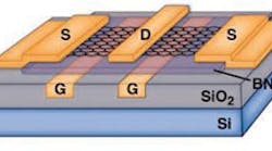
One of the shortcomings of GFETs (see figure) has been the disparity between fT and fMAX performance levels, with fMAX typically being only one-tenth the fT, or an fMAX/fT ratio of 0.1. The columbia and IBM researchers have strived to increase that ratio, and thus the fMAX performance, by using high-quality boron-nitride gate dielectrics. With this approach, they achieve fMAX performance levels as high as 34 GHz for a 600-nm device, with fMAX/ fT ratios as high as 0.86.
By performing S-parameter measurements through 40 GHz with the aid of open-short de-embedding methods, the researchers characterize the forward and reverse transmission characteristics of their GFETs. From their current-gain and unilateral power-gain measurements, they derive an fT of 44 GHz and an fMAX of 34 GHz for their device. By developing a small-signal model based on the measured data, they also predict that fMAX performance can be improved to 58 GHz by means of channel doping and/or gate optimization.
In one notable presentation, Shu-Jen Han and team from IBM will present results on the fabrication of graphene passive devices formed on a 200-mm wafer using a standard CMOS-compatible silicon foundry process. Their work involves the integration of graphene FETs with passive devices to form simple graphene ICs for the first time.
One of the challenges in forming graphene devices is establishing a high-quality atomic-layer-deposition (ALD) or chemical-vapor-deposition (CVD) gate dielectric on the material's inert surface, as required for both FETs and passive circuit structures. CVD-grown graphene is unique because it can be transferred onto almost any substrate, including wafers with predefined embedded gate structures. This can eliminate the need for depositing a dielectric layer on the graphene material. The use of embedded gates allows extremely thin dielectric layers to be employed for reduced gate resistivity and improved high-frequency performance.
The IBM team uses CVD to monolithically integrate graphene FETs and graphene passive circuit elements, forming the first known GHz-frequency-range graphene ICs. Although these ICs are extremely simple, they demonstrate the feasibility of the IBM graphene fabrication process. As an example, a four-turn inductor has been monolithically integrated with a sixfinger graphene FET and the fabricated IC characterized as an RF frequency doubler. The simple circuit exhibited 25 dB conversion gain, with input and output frequencies of 1 and 2 GHz, respectively.
Graphene is viewed by many to be a future building-block material for future nanoelectronic devices, especially for RF applications. Sub-100-nm graphene FETs have been reported with fT as high as 150 GHz. But phonon scattering within the FET devices can play an important role in limiting RF/microwave performance, and can even introduce self-heating effects.
For this reason, accurate modeling is essential to exploring the potential use of graphene device technology for RF/microwave applications. Yang Lu and Jing Guo from the University of Florida (Gainesville, FL) have focused their research efforts on a dissipative quantum transport simulator for graphene transistors. Their software is designed to model Klein band-to-band tunneling and dissipative phonon scattering processes in short-channel graphene transistors.
Simulating a graphene FET with a channel length of 100 nm, gate oxide thickness of 3 nm, and dielectric constant of 20, they have explored the connections between phonon scattering and the DC and RF performance of a graphene FET. They have found that at high drain bias, highenergy phonon scattering can back-scatter electrons, causing them to return to the source because of the lack of a bandgap in the graphene material. This scattering effect can result in low device ballisticity and degraded RF/microwave performance. By simulating suppression of high-energy phonon scattering, ballisticity has been shown to improve, demonstrating the importance of phonon engineering as part of the design of GFETs.
