Download this article in PDF format.
Electronically steerable antennas are gaining favor in radar, communications, and satellite communications (satcom) applications due to several key benefits. The capability to re-position an antenna quickly, the availability of low-profile designs, and longer operating lifetimes continue to make active electronically steered antennas (AESAs) attractive choices compared to mechanically steered dish antennas.
All of these applications require a transmit and receive function with gain and phase controls that can significantly increase the size of the antenna with many radiating elements. However, that’s not the case with the ADAR1000 active antenna integrated circuit (IC) developed by Analog Devices. This four-channel X/Ku-band antenna beamforming chip provides 31-dB gain from 8 to 16 GHz with full 360-deg. phase control. It also includes dedicated memory and power detectors for ease of use. All that in a 88-pin LGA package measuring just 7 × 7 mm.
TDD and FDD
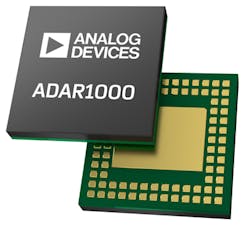
The ADAR1000 (Fig. 1) isn’t simply an active antenna chip—it’s a programmable antenna array in a miniature chip-sized package that enables four channels of efficient transmission and reception across its wide frequency range. It supports time-division-duplex (TDD) operation, replacing as many as 12 discrete components for antenna phase and gain adjustments from 8 to 16 GHz.
1. The ADAR1000 active antenna beamforming chip provides the operation of the receiving and transmitting of the cycle from 8 to 16 GHz.
The chip also can be configured to work in a frequency-division-duplex (FDD) system, such as a satcom application, by running the transmit (Tx) function only in one IC and the receive (Rx) function only in a second IC, powering off the unused portion of the circuit. The densely packed active circuit is fabricated in a commercial SiGe BiCMOS semiconductor process with high repeatability.
The ADAR1000 may simplify the design of communications systems antennas, but it does not sacrifice performance. It maintains gain flatness of typically ±1 dB for any 1-GHz bandwidth between 9 and 14 GHz, with gain flatness of typically ±2 dB from 9 to 14 GHz and typically ±3 dB from 8 to 15 GHz. The gain variations with temperature are typically ±3.5 dB for operating temperatures from −40 to +85ºC.
Four power detectors in the IC have 30-dB detection ranges; an 8-b analog-to-digital converter (ADC) can be used with the power detectors and temperature sensor. It even includes bias and control circuitry for use with external Tx/Rx modules to further simplify the design process.
With its high level of integration, the four-channel ADAR1000 active antenna beamforming chip supports communications, surveillance, and next-generation radar systems. The gain and phase of all four receive and transmit channels can be independently programmed for flexibility, with settings stored in built-in memory or external memory for ease of access and construction of multiple-channel antenna configurations.
In receive mode, the four Rx input signals are combined to a common RF input-output (IO) package pin. In transmit mode, the RF IO signal is divided into four Tx signals for transmission. The better than 6-b digital resolution results in gain resolution that’s finer than 0.5 dB and phase resolution better than 2.8 deg.
A four-wire serial programming interface (SPI) provides control of the on-chip registers for the ADAR1000. In receive (Rx) mode, the four Rx inputs are combined to a common RF_IO pin. In transmit (Tx) mode, the RF_IO signal is split into n additional signals, with two address pins to allow software selection of one out of four core chips on the same serial lines. Furthermore, dedicated Tx and Rx load lines provide synchronization of all core chips in the same array, and a single TR pin enables very fast switching between transmit and receive modes.
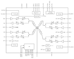
The ADAR1000 accomplishes time-division-duplex (TDD) operation by means of four identical transmit/receive (Tx/Rx) channels (Fig. 2). Each Rx channel has its own low-noise amplifier (LNA) as well as a phase shifter and a variable-gain amplifier (VGA). Each Tx channel has a VGA followed by a phase shifter and a driver amplifier (Fig. 3).
2. The beamformer IC accomplishes TDD operation by means of four identical Tx/Rx channels.
3. An active vector modulator architecture helps achieve phase control where needed in the ADAR1000 system.
The Tx or Rx signal path is selected by means of a high-speed Tx/Rx switch. An attenuation stage with switched 0- or 15-dB attenuation is included in the Tx/Rx common path between the Tx and Rx modes before connecting to a passive 4:1 combining/dividing network. Gain control is provided for each channel to compensate for the effects of temperature and processing, and to be able to taper the beam for low side-lobe levels.
In terms of density, the ADAR1000 is more like a system than a device, packing in the aforementioned temperature sensor, 30-dB power sensors, and ADC. It accomplishes amplitude control though a combination of independent Rx and Tx path VGA adjustments, which provide a gain control range of more than 16 dB, and a switched 0/15-dB attenuator shared between the Tx and Rx channels. The amplitude control range between the two devices is effectively more than 31 dB.
A total of 8 b of digital control is used by either the Rx or Tx channel for amplitude control. The VGAs require 7 b of control to ensure a minimum step size of 0.5 dB with less than 0.25-dB error for all operating conditions. The eighth bit controls the state of the switched attenuator. A portion of the amplitude control range would typically be used to compensate the channel gain for temperature, process variations, and amplitude variations in the phase shifter as a function of phase setting. The remaining portion of the control range can be used for other amplitude control functions, such as tapering for side-lobe control.
Beyond its flexibility and programmability, the ADAR1000 features power-saving bias modes. It’s designed to simplify the addition of antennas, at least to the frequency range of 8 to 16 GHz, without occupying too much of an electronic product’s total package. In addition to easing the design process, it provides a generous number of options in terms of final product size, weight, and power (SWaP), without overly sacrificing product performance.
Analog Devices Inc., One Technology Way, Norwood, MA 02062; www.analog.com


