Designing a Step-Recovery-Diode-Based Comb Generator
Download this article in PDF format.
The task of designing frequency multipliers and comb generators has traditionally been plagued by challenges such as low output power, unexpected parasitic frequencies, and oscillations. Computer-aided-design (CAD) software can overcome these problems, though. The purpose of this work is to predict the behavior of a nonlinear step-recovery diode (SRD) in a harmonic-generator circuit. By doing so, one can achieve high correlation between simulation results and measured data.
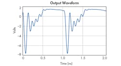
A post-processing display of the harmonically rich output frequency spectrum was produced with Microwave Office software. Output harmonics and their respective magnitudes were graphically displayed for a given single input frequency. In addition, the output waveform on a time scale was examined.
Circuit Design
Microwave Office software was used to design a complete comb circuit and fabricate several circuits. The test results fully agree with the computer-predicted output spectrum. The output power of each harmonic was measured, demonstrating agreement with the simulated results. The output spectrum displays 12 harmonics with no spurious frequencies or oscillations.
The SRD was selected for this design due to its nonlinear properties and ability to attain good higher-order frequency multiplication and fast pulse generation. It takes advantage of its diffusion capacitance for charge storage, resulting in a fast snap time. This design employs an input lowpass filter to provide an impedance match to the diode.

While most multipliers utilize an output “ringer” bandpass filter to suppress the undesired harmonics, this design exploits all of the generated harmonics—a wide range is required. This simplifies the design considerably, making it low cost and easy to manufacture.
The nonlinear behavior is described in the diode model provided by the Microwave Office component models list. The model properties are manually set to the appropriate values consistent with the published Metelics (now MACOM) diode that was selected for this design.
Diode Properties
Multiplier (and comb generator) circuits are reactively terminated at the higher-order harmonics at the output port. Consequently, the power is partially reflected and recombined to produce stronger harmonics. The damping factor of the SRD is one of the primary drivers in frequency-multiplier or comb-generator design. It is defined as follows:
Ï = (1/2RL)(L/Cd )1/2
where L is the diode’s inductance, Cd is the diode’s reverse capacitance, and RL is the load resistance.
A good practical range for the damping factor (Ï) is between 0.4 and 0.5. If damping is too low, stability problems can arise. If it is too high, the output pulse will become too long.
Other parameters important in diode selection are reverse breakdown voltage (Vb), reverse capacitance (Cd), minority carrier lifetime (τn), and transition time (Tt).
In a good multiplier or comb-generator design, Tt should always be less than the output pulse length (Tp), defined as:
Tp = π/ωn
where ωn is the input frequency.
The carrier lifetime must be sufficiently large to allow for recombination while the diode is charging. A practical guideline is:
τn > 10/Fin
where Fin is the input frequency.
The carrier lifetime (τn) should also be long enough for the reverse current to accumulate a high charge level. Then, when forward-biased, an extremely fast “snap” into its high impedance state creates the harmonically rich output.
The diode thermal resistance θjc value is required in order to determine the operating diode temperature. The temperature rise above the baseplate temperature is:
ΔT = (θjc)(Pin)
Diode Selection
The MMD 840-C11 diode was selected for this design. Its published parameters are:
• Breakdown voltage: 15 V
• Diode capacitance: 0.2 to 0.4 pF
• Carrier lifetime: 15 ns
• Transition time: 35 ps
• Thermal resistance: 60°C/W
A good compromise is achieved among the diode’s parameters, making it a good candidate for this application. The vendor supplied the detailed Spice property values that were entered into the library model.
Comb-Generator Circuit Design
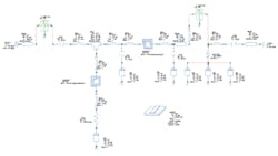
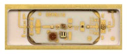
The schematic and circuit layout are shown in Figs. 1 and 2, respectively. All of the circuit elements used in the optimization of this design can be seen in the schematic. All connecting wires, ground via holes, circuit layout details, and material properties were included in the circuit model. The inductor manufacturer supplied the Spice parameters used for the spiral inductors. The circuit was tuned and optimized so that all harmonic signals up to the 12th harmonic are strong. The circuit was constructed on a 15-mil-thick alumina substrate with a dielectric constant of 9.9.
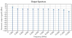
In terms of simulation, Fig. 3 shows the computer-predicted harmonic signal levels. Figure 4 presents the output waveform that displays the “snap” action.
Testing
Ten circuits were constructed and measured. The data is consistent with the predicted harmonic levels. All of the circuits functioned immediately upon first-time power “turn-on.” This was gratifying and is a tribute to the Microwave Office software. No time was spent troubleshooting the circuits for unexpected problems like instability, i.e., output breakups into triangular “Christmas tree” spectrums. Circuit performance was stable and tested predictably over a temperature range of –40 to +85°C.
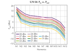
Extensive testing and characterization were performed on two circuits, serial numbers 03 and 04. These were both measured over a wide range of temperatures: –40, +5, +25, +50, and +85°C. In addition, the input power levels ranged from +19 to +28 dBm. Ambient temperature testing was performed on the remaining eight circuits.
The circuits were then transitioned into production. The test data of all circuits is consistent with the data presented in this article. Figure 5 presents graphical data of the measured comb-generator circuit (serial number 04).
Conclusion
A comb generator was successfully created using nonlinear simulation techniques. The implemented topology supported the creation of multiple harmonics from a single diode. The measured results are in close correlation with the simulated values. Several comb generator circuits were fabricated during the design phase. Consistency among each of the circuits validated the design’s robustness. Thus, the usage of the Microwave Office nonlinear simulation software resulted in a comb-generator circuit design that accurately predicted 12 harmonics.
Acknowledgement
I would like to thank Joe Wong and Chung Ly for their prior work and insights on comb generators. Joe Wong did the very early designs, and Chung Ly worked with me in accomplishing this work.
Kimberly Renee Alvarez is a consultant at www.microwaveandrfconsulting.com.
References:
Wayne Thomas, R. Clayton Smith, and Kipp Schoen, “Comb Generator with excellent harmonic flatness to 40 GHz,” Picosecond Pulse Labs, Boulder, Colo., 80301
“Pulse and waveform generation with step recovery diodes,” Agilent application note 918.
“Harmonic Generation using step recovery diodes and SRD modules,” Agilent application note 920.
George H. Stauffer Jr., “Spice up the development of a step recovery diode frequency multiplier,” RF Design, June 1999.
About the Author
Kimberly Renee Alvarez
Independent Consultant
Kimberly Renee Alvarez is an independent consultant working as a contracting engineer. She has worked as an RF engineer at several organizations including Teradyne, L3 Technologies, Rockwell Collins, Southwest Microwave, Tampa Microwave, Raytheon, and Northrup Grumman. She holds a BSEE from West Coast University.
