50-V GaN HEMTs Power LTE Networks
Cost-effectively boosting radio signals at high power levels is critical to the long-term financial health of cellular communications. Cree, Inc. looks to have made some significant steps in the right direction with the introduction of its new +50-VDC gallium-nitride (GaN) high-power devices. The high-electron-mobility-transistor (HEMT) devices provide output-power levels of 100 and 200 W at frequency bands from 1.8 to 2.2 GHz and 2.5 to 2.7 GHz. They also boast the high efficiency needed by Fourth-Generation (4G) Long-Term-Evolution (LTE) cellular base stations for real savings in cellular network operating costs. A large portion of the power required by a cellular base station is consumed by the transmit power amplifier, so any improvements in transistor drain efficiency will translate into significant savings in operating costs.
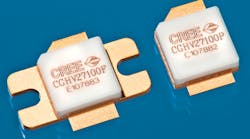
Cree’s new 50-V GaN HEMT devices include 100-W models CGHV22100F and CGHV22100P in flange- and surface-mount ceramic-metal housings (see figure), respectively, for applications from 1.8 to 2.2 GHz. Also included are 100-W models CGHV27100P and CGHV27100F in flange- and surface-mount ceramic-metal housings, respectively, for applications from 2.5 to 2.7 GHz. In addition, the company also announced the availability of 200-W models CGHV22200F and CGHV22200P for 1.8 to 2.2 GHz, and 200-W models CGHV27200P and CGHV27200F for use from 2.5 to 2.7 GHz. Each device is internally impedance matched for its frequency band and supplied in rugged ceramic/metal housings with excellent thermal dissipation.
Models CGHV22100F and CGHV22100P, for example, provide typical gain of 20 dB from 1800 to 2200 MHz, with gain levels of 18.7 dB at 1800 MHz, 20.7 dB at 2000 MHz, and 22.0 dB at 2200 MHz when delivering +44 dBm output power into a Cree amplifier test fixture. The 100-W GaN transistors offer very respectable linearity, judging by adjacent-channel-leakage-ratio (ACLR) performance of -37.8 dBc at 1800 MHz, -37.1 dBc at 2000 MHz, and -35.1 dBc at 2200 MHz. At +44 dBm output power, the drain efficiency is 35.4% at 1800 MHz, 31.7% at 2000 MHz, and 30.6% at 2200 MHz.
With twice as much output power, models CGHV22200F and CGHV2200P are flange- and surface-mount packaged devices, respectively, with 16.6 dB gain at 1.8 GHz, 19.2 dB gain at 2.0 GHz, and 18.1 dB gain at 2.2 GHz. These 200-W GaN transistors offer drain efficiency of 31.5% at 1.8 GHz and +47 dBm output power, 31.9% at 2.0 GHz and +47 dBm output power, and 34.8% at 2.2 GHz and +47 dBm output power. For +47-dBm output power, they achieve ACLR of -37.4 dBc at 1.8 GHz, -37.4 dBc at 2.0 GHz, and -35.6 dBc at 2.2 GHz.
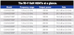
For higher-frequency LTE base-station applications, models CGHV27100F and CGHV27100P are flange- and surface-mount-packaged GaN HEMTs, respectively, rated for 100 W output power from 2.5 to 2.7 GHz. Meanwhile, models CGHV27200F and CGHV27200P are GaN HEMTs with 200-W output-power capability from 2.5 to 2.7 GHz (see table). The 100-W devices deliver 18.0-dB typical gain with -37 dBc ACLR and 33% drain efficiency at 25 W average output power. At +44-dBm output power, these GaN power transistors provide 18.1-dB gain at 2.5 GHz, 18.0-dB gain at 2.6 GHz, and 17.9-dB gain at 2.7 GHz. At that output-power level, the drain efficiency is typically 34.0% at 2.5 GHz, 33.5% at 2.6 GHz, and 32.0% at 2.7 GHz, while the ACLR is typically -37.0 dBc at all three test frequencies (2.5, 2.6, and 2.7 GHz).
The 200-W transistors achieve 16-dB typical gain from 2.5 to 2.7 GHz, with -37 dBc ACLR and 29% drain efficiency at 40 W average output power across that 200-MHz bandwidth. At +47-dBm output power, these devices offer 15.0-dB gain at 2500 MHz, 16.0-dB gain at 2600 MHz, and 16.0-dB gain at 2700 MHz. The drain efficiency at that output level is 29.0% at 2500 MHz, 28.5% at 2600 MHz, and 29.0% at 2700 MHz, while the ACLR is -36.5 dBc at 2500 MHz, -37.5 dBc at 2600 MHz, and -37.0 dBc at 2700 MHz.
As with the lower-frequency, lower-power transistors, the GaN HEMTs are evaluated in a Cree amplifier test circuit using WCDMA 3GPP test conditions. All of these packaged GaN HEMTs are durable, designed to handle mismatch stress equivalent to a 10.0:1 output VSWR. All are rated for maximum operating junction temperature of +225°C, maximum drain-to-source voltage of +125 VDC, and case operating temperature range of -40 to +85°C.
CREE, Inc., 4600 Silicon Dr., Durham, NC 27703; (919) 407-5639, www.cree.com/rf

