Managing Phase Noise In Microwave Sources
Phase noise haunts every high-frequency signal source at some level. Though it can be minimized through attention to careful design practices and use of good materials, it cannot be eliminated. Phase noise is basically the short-term, random fluctuations of frequency in a signal source, such as an oscillator, frequency synthesizer, or test signal generator. Because some amount of phase noise is inevitable in a high-frequency source, it may be helpful to reach some understanding on what levels might be considered acceptable, and what the effects of phase noise on a system are if those levels are too high.
An ideal RF/microwave signal source such as a transistor oscillator would generate an output signal with no fluctuations in frequency or phase, and no noise at the output. If tuned to a particular frequency, the source would remain at that frequency over time, without drift or other variations. Unfortunately, not only will it drift in frequency over long periods of time, but it will also suffer short-term variations in frequency—what we know as phase noise.
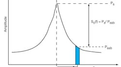
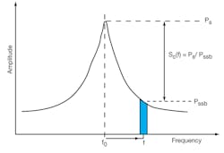
If an oscillator’s output signal is visualized as the amplitude peak of a sine wave, both lower and upper sidebands of the signal contain noise. A source’s phase noise can be characterized for one or both sidebands as single-sideband (SSB) or double-sideband (DSB) phase noise, respectively. Nonetheless, most commercial oscillators, signal generators, and other high-frequency signal sources are specified and compared according to their SSB phase noise, which can be represented on a diagram showing the peak amplitude and the measurement bandwidth for the noise at some offset distance from the carrier. As the shape of the carrier plot shows (Fig. 1), the phase noise will decrease as the offset from the carrier increases.
1. This diagram illustrates the carrier portion of a sine wave and the definition of single-sideband (SSB) phase noise referenced to a 1-Hz measurement bandwidth. (Diagram courtesy of Mini-Circuits.)
In this plot of phase noise, borrowed from the application note from Mini-Circuits, “VCO Phase Noise,” Ps represents the signal or carrier power; Pssb is the single-sideband power in a 1-Hz bandwidth at some offset distance from the carrier; f0 is the carrier center frequency; and Sc(f) is the phase noise or power density in one sideband per Hz of bandwidth at an offset frequency, f, from the carrier. As this plot shows, the phase noise is basically the ratio of the noise power in a 1-Hz bandwidth at a specified offset from the carrier to the carrier signal power, given in dBc/Hz. Phase noise in the frequency domain corresponds to jitter in the time domain.
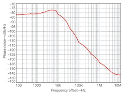
As a standard SSB plot of phase noise indicates (Fig. 2), the noise level diminishes as the offset frequency from the carrier increases. The phase-noise offset frequency is often referred to as either “close-in” phase noise or phase noise that is far from the carrier. Both terms can be somewhat arbitrary in nature, with close-in phase noise typically referring to noise at offset frequencies of 100 Hz or less, but often including offset frequencies to 1 kHz. Phase noise that is far from the carrier usually refers to offset frequencies of 1 MHz or greater.
2. This is a standard plot for displaying SSB phase noise at various offsets from the carrier. (Diagram courtesy of Analog Devices.)
The location of the phase noise can have significance for different applications. For example, in signal-sampling applications using an analog-to-digital converter (ADC), close-in phase noise on the clock oscillator can cause errors in sampling an input signal’s frequency. The phase noise that is further from the carrier, also known as broadband noise, will cause degradation in the overall signal-to-noise ratio (SNR) of the signal sampling system or circuit.
Many factors can affect phase-noise performance in an RF/microwave source, including the materials used in a resonator, the type of active device in an oscillator, and the reference oscillator used in a frequency synthesizer. Noise on the power supply to the oscillator, for example, can translate to phase noise at the output of the oscillator. For optimal phase-noise performance, an oscillator’s active device should exhibit low noise figure as well as low flicker noise.
An oscillator’s phase noise will inevitably be limited by thermal noise, NT, which is caused by the Brownian motion of electrons due to thermal agitations. Thermal noise is often represented by the simple expression:
NT = kTB
where:
k = Boltzmann’s constant;
T = the temperature in degrees Kelvin, or 290 K at room temperature, or +17°C); and
B = the bandwidth.
At room temperature or 290 K, NT = -174 dBm/Hz.
A low-noise oscillator, such as a crystal oscillator, will also exhibit a noise floor which can serve as a limitation in measuring the phase noise of other oscillators, since low-noise oscillators are often needed as a reference source for measurements. The noise floor for a low-cost crystal oscillator may be about -150 dBc/Hz versus about -160 dBc/Hz for a good low-noise version.
Test systems and spectrum analyzers
For measuring source phase noise, a number of companies offer dedicated (and sophisticated) test systems, such as the PN9000 phase-noise measurement system from Noise XT, the E5500 series of phase-noise measurement systems from Agilent Technologies, and the BluePhase 1000 phase-noise test system from Wenzel Associates. These systems typically combine a number of different function modules—such as phase detectors, local oscillators (LOs), and power supplies—to achieve a specified measurement performance level.
Some of these systems deliver carrier coverage well into the millimeter-wave frequency range using additional frequency translators and harmonic converters. The PN9000 and E5500 systems offer measurement capabilities at offsets as close as 0.01 Hz to as far as 1 MHz, in the case of the PN9000, and 100 MHz for the E5500 systems. The E5500 systems boast a noise floor of -180 dBc/Hz. The BluePhase 1000 system offers more humble performance levels, working across an offset range of 1 Hz to 100 kHz for carrier frequencies from 5 MHz to 1.5 GHz, but still with an impressive noise floor of -178 dBc/Hz offset 10 kHz from the carrier.
Of course, measuring phase noise can be as simple as using a spectrum analyzer, provided that its internal noise is low enough. Most instrument makers recommend that a spectrum analyzer have phase-noise characteristics that are at least 10-dB better than an oscillator or signal source to be measured. Ideally, the analyzer also includes resolution-bandwidth filters narrow enough to measure the noise power in a 1-Hz measurement bandwidth.
The spectrum analyzer should also provide sufficient measurement dynamic range to display the level of a carrier of interest, as well as the low noise levels far from the carrier (or at least at offsets from the carrier that are important to the measurements). A simple way to check whether a spectrum analyzer’s thermal noise will interfere with a phase-noise measurement is to compare noise levels at an offset of interest with and without the source to be tested connected to the analyzer’s input port. A clear difference in the noise levels at the offset of interest usually indicates that the analyzer’s thermal noise will not be a problem for phase-noise measurements made with the analyzer.
It is also critical when measuring phase noise with any system that the impact of external energy sources be minimized. To minimize external noise effects—especially at the low levels being measured—it may be necessary to enclose the source under test in some form of a shielded enclosure, and to use coaxial cables with high shielding effectiveness (SE) of 100 dB or better to minimize the possibility of the connecting test cables acting as an antenna for external energy sources. The power supply for any test setup should also be properly screened to minimize noise.


