High-Power Switched Filter Banks Raise the Temperature of Design Challenges
This file type includes high resolution graphics and schematics when applicable.
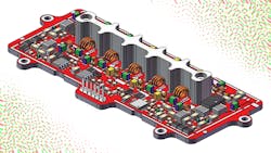
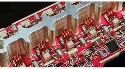
Switched filter banks (SFBs) are traditionally found in RF front ends or intermediate stages of sensitive receivers for military and defense applications, as they help reduce harmonic and spurious content which is critical to communications systems. Until recently, high-power SFBs (Fig. 1) have been limited to fixed locations or on larger mobile platforms due to their inherent large size.
Gallium-nitride (GaN) power amplifiers (PAs) have reduced the size and weight of high-power transmitters in the hundreds of watts range. The demand for SFB assemblies has thus followed suit. However, the leap from traditional SFBs to high-power equivalents is not straightforward, and many tradeoffs and design considerations must be made in order to develop a suitable high-power SFB.
One application that has driven the early development of high-power SFBs is communications band signal jamming at VHF and UHF frequencies. These devices have predominantly been used to prevent communications band signals to remotely triggered explosives and to deny cellular service near secure governmental and military facilities. Ironically, technology that has initially been leveraged to mitigate communications may be a solution that enhances communications in modern and future trending applications.
Practical Justifications for High-Power SFBs
As communications band usage increases with the explosion of the Internet of Things (IoT) and machine-to-machine (M2M) devices, there may be greater commercial and industrial sector demand for high-power amplification and switching technology that limits the spurious content in these bands. A reason for this is that any additional harmonics or spurious content could dramatically increase the interference and noise to nearby low-power IoT/M2M systems.
For example, the latest autonomous (or connected) car may heavily rely on a constant communication channel to a common base station and between other vehicles for safe operation. In a world with a densely packed web of critical systems, cranking up the transmitter power won’t be an option to preserve reliable communications. Thus, the high-power systems in heterogeneous networks may require more stringent operational specifications.
Another future application of high-power SFBs could be enabling high-speed communications channels for commercial and industrial drones. The adoption of unmanned aerial systems (UAS) technology is accelerating and may play a larger role in commercial and industrial applications. The reliable control and communication with these systems will require more agile and small payload radio technology, possibly served by high-power SFBs coupled with the latest high-power amplifiers (HPAs).
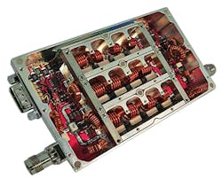
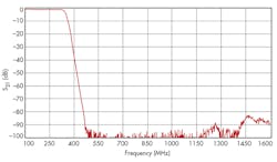
At API Technologies, high-power filter bank solutions have been developed to filter the high-power signals generated by PAs. There are several constraints that must be considered when developing high-power SFB solutions, which include the pass-band, applied power, reflected power, switching speed, and the stop-band region (Fig. 2).
The Differences Between High-Power and Low-Power SFBs
High-power SFBs are generally judged by the same performance parameters as lower-power SFBs: among them, size, weight, and cost. Electrical considerations, such as passband, roll-off, insertion loss, and out-of-band rejection are also just as significant in high-power SFBs. Achieving a lower insertion loss and higher out-of-band rejection may require more design effort for high-power SFBs, as heat dissipation from a high insertion loss and attenuating high power harmonics are often key considerations.
The main differentiations between low-power and high-power SFB requirements include high-power SFBs’ heat dissipation characteristics and the high voltage handling needs. These two factors of high-power operation induce greater voltage and thermal stresses on the switch elements and components directly in the signal chain. Additionally, higher voltages and power increase the impact of nonlinearities in system components. These factors demand a detailed analysis of each component’s performance over a wide range of operational parameters.
High-Power SFB Design Challenges
The SFB is often considered a less-critical component than an HPA system. However, an assembly that wasn’t designed upfront with the considerations of the SFB may lead to an underutilization of the amplifier module’s capability or significant amounts of costly redesign. It is therefore important to consider the high-power SFB as a critical item in the assembly.
The physical demands by the latest applications also encourage much lower size, weight, and reduced cost structure without sacrificing functionality. This is hard to achieve without optimizing the physical and electrical design of the SFB section in an integrated assembly. The power and thermal factors also form a trade-off with frequency and bandwidth, as high-frequency RF signals tend to generate greater thermal dissipation in signal chain components in much smaller dimensions.
Additionally, high power, voltage, current, and thermal stresses can exceed the maximum operating specifications for many components not designed specifically for high-power operation. A complete understanding of the signal characteristics presented to the assembly establishes design requirements so that each component can be optimized to withstand the various stresses associated with the applied power. For example, various continuous and pulsed power conditions can dramatically influence the thermal consideration and transient voltage/current handling parameters of many signal chain components.
Another electrical consideration is the increased harmonics from nonlinear components whose harmonic products scale with input power. The active switching elements—such as PIN diode and FET switches—fall under this category, as does any nonlinear driver and bias circuitry. Higher RF power also leads to increased reverse bias voltages that can affect diodes, drivers, resistors, and interconnect components. This in turn increases the thermal stresses experienced by those components. The switching speed is also limited by the power and thermal stresses experienced during switching.
Component/Device Limitations and Considerations
Every component and device in the signal chain of a high-power SFB also brings limiting factors, parasitics, and design challenges. For example, switches and inductors are critical to design performance. For inductors, the ability to carry high RF power requires an increase in wire thickness to minimize thermal concerns from resistive losses. An increase in wire diameter also increases the parasitic capacitances—interwinding capacitance and shunt capacitance to nearby grounds—and overall inductor size and inductance, which ultimately limits the diversity of filter topologies and quality factor of the filter stage.
The switches in a high-power SFB are burdened with the twin tasks of allowing and blocking hundreds of watts of RF power without exceeding power, voltage, current, and thermal operating parameters. For these reasons, it is generally infeasible to achieve the necessary device performance while enabling hot-switching capability. Hot switching would induce potentially significant transients that could easily exceed the switch device ratings, or even the PA and downstream components.
Specifically for PIN diode switches in a high power SFB, hot switching poses a hazard to itself and other components and devices. During a PIN diode on-state, the insertion loss through the switch is very low; in the off-state, the PIN diode has a very high resistance and low leakage current. However, while a PIN diode is switching, the impedance during the transitional state can cause the switch to dissipate the bulk of the applied power resulting in failure of the diode (Fig. 3). Thermal energy induced during hot-switching could also exceed the switch materials operating parameters, leading to accelerated aging or device failure.
The Big Thermal Challenge
Though understanding the magnitude of RF energy converted to thermal energy in a high-power signal chain is relatively straightforward physics, managing the thermal energy in such a way that prevents device/component failure and undesired operation is a far greater challenge. As sustained high temperatures can influence performance, accelerate aging, and even destroy components/devices, appropriately designing and testing a high power SFB assembly can ensure longevity and proper operation, even under environmental extremes. In many cases, an assembly is tested under extreme temperature conditions to determine whole assembly survivability.
However, extreme temperatures may not occur or affect each component in an assembly in the same way. These factors may require rigorous and individual device and component testing while thermal cycling to discover failure modes and limitations. Understandably, this level of consideration applies to applications where failure of the assembly in the field is worth the added upfront expense of such rigorous performance analysis.
At API Technologies, to avoid failures from thermal breakdown, every high-power design is examined with an infrared camera while under worst-case operational conditions to determine which, if any, components are exceeding their maximum operational temperatures. Typically, if a component is within 15-20% of the maximum operational temperature they are examined more closely and mitigation actions are taken. In some cases, the company requires the part be tested 100% while being examined with the camera to ensure that those parts do not exceed the operational temperature.
Other methods of optimizing a design with thermal considerations include using 3D CAD models in both electromagnetic (EM) simulators and thermal simulators to predict areas of thermal concern early in the design phase. With some details known about the high thermal stress areas in the design, changes to the thermal management system of the assembly can be made in early stages of the design cycle—where costs for modifications tend to be less expensive.
Computer modeling and simulations have advanced significantly in the past few years (Fig. 4). Nevertheless, these design tools cannot replace an engineer’s design experience and understanding of the complex interactions between system components. Additionally, a trained eye is extremely valuable in interpreting the modeling and simulation data, then converting that information into design solutions.
The complex design challenges associated with providing reliable and high-performance filtering for the latest high-power applications has brought about many creative and unconventional solutions when compared to a traditional SFB. Producing drop-in SFB modules that leverage standard high volume assembly methods is one approach to reducing the size, cost, and manufacturing time of previous sophisticated custom-made hardware. Future communications technology trends—along with increased commercial, industrial, and military demand for high-power SFB technology—will continue to require design and system engineers to push the boundaries of filter assembly design.
Jon Scoglio, Engineering Manager
References & Resources
MEMS-based Amplified Switch Filter Bank
High Performance Switched Filter Banks
Looking for parts? Go to SourceESB.
This file type includes high resolution graphics and schematics when applicable.
