GaN Breaks Through Performance Barriers
This file type includes high-resolution graphics and schematics when applicable.
Gallium-nitride (GaN) technology has officially arrived, as applications ranging from defense to commercial cellular exploit its performance benefits—benefits that are simply unavailable with older semiconductor technology like gallium-arsenide (GaAs). Today, a number of different suppliers offer an array of GaN devices. And GaN shows no signs of slowing down, as it will likely find its way into more future applications. So expect the GaN train to keep rolling along, with suppliers continuing to develop and deliver new cutting-edge GaN products.
Aerospace and Defense
Aerospace and defense applications undoubtedly reap the benefits of GaN technology. “GaN is changing the RF and microwave landscape for aerospace and defense systems, with almost all future radar, military communications, and electronic-warfare (EW) systems investigating the benefits,” says Mike Scott, senior business development manager for modules and subsystems at Analog Devices. “By reducing device parasitic elements and using shorter gate lengths and higher operating voltages, GaN transistors have achieved higher output-power densities, wider bandwidths, and improved dc-to-RF efficiencies.”
Phased-array radar is just one example of an application that benefits from GaN technology. “In modern phased-array radar systems with thousands of active elements, our GaN technology is providing comprehensive solutions for transmit/receive (T/R) modules,” he continues. “Both power density and integration are increased, with the power amplifier (PA), low-noise amplifier (LNA), and T/R switch all developed in GaN. The high breakdown voltage also potentially mitigates the need for the limiter, which is traditionally used to protect the LNA. Thus, component count and area are reduced, which is critical at higher frequencies with minimal antenna aperture spacing.”
Utilizing GaN technology can help designers satisfy the goal of delivering superior performance in a small package size. “The size of modern-day systems is becoming an ever more important issue,” says Scott. “The improved power density of GaN is as much as six times greater than GaAs. Therefore, GaN can enable reduced system footprints with higher reliability.”
Wider bandwidth capability, as mentioned, is another of the key performance enhancements offered by GaN. Scott notes, “Higher operating impedances also provide optimized solutions for electronic surveillance and countermeasures, as a single broadband PA can now cover multi-octave bandwidths. For example, our HMC7149 PA, which is based on a 0.25-μm process, can provide amplification across a frequency range of 6 to 18 GHz with minimal variation of output power and gain.”
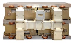
Power-combining solutions are incorporated with GaN in Analog Devices’ new high-power amplifier modules, which the firm says offer a reliable alternative to traditional traveling-wave tubes (TWTs) (Fig. 1). “Using proprietary power-combining methods and advanced bias-control/monitoring circuits in core power-combined modules, our solid-state high-power amplifiers (SSHPAs) range from 100-W broadband amplifiers to 8-kW X-band amplifiers, combining as many as 256 monolithic microwave integrated circuits (MMICs),” adds Scott.
Wireless Infrastructure
The impact of GaN extends well beyond aerospace and defense applications. Commercial cellular networks are also capitalizing, with many wireless base stations now turning to GaN. Laterally diffused metal-oxide semiconductor (LDMOS) technology has dominated the wireless infrastructure arena for some time. However, GaN has clearly made inroads into this market, and seems destined to make a greater impact in this arena.
One of the players in the GaN space is Qorvo, which offers a large number of devices that cover frequencies ranging from dc to Ka-band. The company is at the forefront of GaN-on-silicon-carbide (GaN-on-SiC) technology, which it sees as a solution for wireless base stations.
“The two leading GaN process technologies today are GaN-on-SiC and GaN-on-silicon (GaN-on-Si),” says Sumit Tomar, general manager of wireless infrastructure at Qorvo. “GaN-on-Si has the advantage of a lower-cost substrate. But that advantage is outweighed by GaN-on-SiC’s support of much greater power density and better thermal management. As a result, GaN-on-SiC has become the natural choice for base stations that require high-power outputs.”
Tomar adds, “The advantages of GaN-on-SiC will become even clearer as operators increase network capacity by using techniques that will require higher power, such as carrier aggregation (CA) and multiple-input, multiple-output (MIMO). Operators are demanding higher power output each year. Last year’s base-station power requirements were at 30 to 40 W, but that number has increased to today’s requirement of 60 W. We can expect as much as 100 W or more in next-generation base stations.
“As GaN PAs become more widely used in LTE networks, careful evaluation of solutions is essential to ensure they can meet the tough requirements placed on network infrastructure. Thus, a significant factor will be the choice between GaN-on-SiC and GaN-on-Si. Product reliability is also essential. It is critical that we keep our eyes on the power demands of our evolving technology—both now and in the future.”
Qorvo currently offers a wide array of GaN devices, such as the recently introduced TGA2218-SM and QPA2237 PAs. The TGA2218-SM PA, which covers 13.4 to 16.5 GHz, provides 12 W of output power. The QPA2237 is a 10-W PA that spans 0.03 to 2.5 GHz. Additional new products include the TGF2977-SM, TGF2978-SM, and TGF2979-SM RF transistors, each of which cover dc to 12 GHz, and provide 5, 20, and 25 W of output power, respectively.
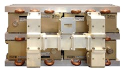
Another company focused on delivering GaN-based solutions to the wireless infrastructure market is MACOM, which recently announced its new MAGb series of GaN power transistors for wireless base stations (Fig. 2). With these new series of transistors, MACOM is proving that GaN-on-Si is a viable technology solution for today’s applications.
“The wireless base-station market is fueling tremendous innovation in GaN technology,” says Preet Virk, senior VP and general manager of the carrier networks group at MACOM. “Base-station original equipment manufacturers (OEMs) are now taking a much closer look at the relative merits of GaN-on-Si and GaN-on-SiC transistors for base-station PAs. These OEMs are assessing the advantages and tradeoffs that range from performance attributes to supply-chain ecosystems. In order to displace LDMOS in the commercial base-station domain, a favorable price/performance balance must also be established.”
Virk adds, “We have addressed this requirement with our new MAGb series of power transistors, which provide GaN-caliber performance at LDMOS-like cost structures. We have also formed a path to better-than-LDMOS cost at scaled volume production levels. Leveraging our fourth-generation (Gen4 GaN) technology, these GaN-on-Si-based transistors have demonstrated efficiency in excess of 70% along with linear gain of 19 dB at 2.6 GHz. Furthermore, they can achieve greater than 80% peak efficiency when the devices are presented with proper harmonic terminations. This power-efficiency profile rivals that of GaN-on-SiC devices, and represents as much as 10% improvement in efficiency in comparison to LDMOS offerings.”
In addition, the company believes these products lend themselves well to digital pre-distortion (DPD) techniques. “Another key challenge that GaN needs to overcome in the base-station domain is the non-linearity that’s common to Doherty amplifier implementations,” says Virk. “This is typically corrected with DPD. However, DPD has proven to be difficult to implement with GaN-on-SiC devices. The charge trapping effects in SiC, believed to be caused by crystalline defects in its silicon structure, ultimately yield PAs that are more difficult to linearize. MACOM GaN does not exhibit the same levels of the aforementioned artifacts, and is therefore easy to linearize and correct with DPD schemes.”
Among other suppliers introducing GaN devices for the wireless infrastructure market is Mitsubishi Electric. The firm recently expanded its lineup of GaN high-electron-mobility-transistors (HEMTs) for 4G base transceiver stations (BTSs). The four new transistors are intended for 3.5-GHz applications, with output-power levels that range from 5 to 180 W. According to Mitsubishi, using these new products can reduce BTS power consumption. The company also boasts that PA modules can be built in smaller sizes when designed with these transistors.
Infineon Technologies entered the fray with its new family of GaN RF power transistors. Cellular amplifiers implementing these new devices can achieve high efficiency and broadband performance, says the company. The 70-W GTVA220701FA transistor covers 1805 to 2170 MHz, while the 170-W GTVA261701FA transistor spans 2620 to 2690 MHz.
More GaN Suppliers
The aforementioned companies are certainly not alone as providers of GaN devices. For instance, Wolfspeed’s GaN devices find homes in applications that include satellite-communications (satcom), radar, and telecommunications. In fact, it was recently announced that the total output power of the GaN-on-SiC RF power transistors shipped by the company exceeds 1.3 GW.
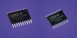
Last year, Wolfspeed released the 60-W CGHV27060MP and CGHV35060MP GaN HEMTs (Fig. 3). The CGHV27060MP covers a frequency range of dc to 2.7 GHz, while the CGHV35060MP spans 2.7 to 3.5 GHz. Both transistors are well-suited for radar and LTE applications.
Also sparking interest is Ampleon, as the company recently extended its portfolio of GaN RF power transistors based on a 0.5-μm HEMT process technology. The CLF1G transistors are currently available in output-power levels ranging from 10 to 100 W. These products, housed in compact and thermally stable ceramic packages, will make their way into applications such as radar and wireless infrastructure, among others.
In addition, Sumitomo Electric Device Innovations offers numerous GaN devices targeting a range of applications. For example, the company recently expanded its offering of satcom products by unveiling both 30- and 60-W Ku-band devices. Additional products are available for other satcom bands, such as C- and X-band. One of the newer devices, the SGK5872-20A, is a C-band device that provides 20 W of output power over a frequency range of 5.85 to 7.2 GHz.
Sumitomo Electric Device Innovations also offers GaN devices for applications like radar. One such product is the SGC8598-200A-R GaN HEMT, which will find homes in X-band radar applications. The device, which spans 8.5 to 9.8 GHz, provides 200 W of output power in pulsed operation.
In the last several years, we have clearly witnessed a shift toward GaN technology. However, despite all of the activity surrounding GaN, the technology is still relatively new. We can expect to see GaN’s capabilities grow, e.g. higher-frequency performance, in the near future as researchers further explore its capabilities. Although older semiconductor technologies are not likely to disappear anytime soon, it does seem apparent that next-generation applications will increasingly turn to GaN as the go-to solution.
Looking for parts? Go to SourceESB.
